Past Research


Over the last decades computing platforms have experienced a drastic reduction in size, and increase in proximity to the user. With the advent of smartphones, this scaling has been limited by the need of a User Interface to allow human interaction. To break this limit, computing platforms are thus moving from being in proximity to the user, to being in proximity to the data source, with the so-called Internet-of-Things (IoT). Such IoT nodes are characterised by a small form factor that strongly limits their battery capacity. This, in conjunction with the need of a long battery life, creates strong constraints on the power consumption of such nodes.

Thus, a lot of effort is being given to the power efficiency of all the components of these nodes. In our laboratory we focus on the optimisation of the always-on timer reference. This, in fact, has to be ultra-low-power, as it is a major contributor to the power consumption of the system when in sleep mode, but also needs to be accurate in order to not waste precious time and power for re-synchronisation during the transmission mode. For these reasons, in our lab we are working on an on-chip reference with high energy efficiency and low PVT sensitivity. Additionally, such reference can be fully integrable, thus removing the need for a bulky 32kHz crystal oscillator, allowing a much easier manufacturing.
Contact


The recent developments in the wireless communication industry, and the constant increase of communication devices have sparked the interest in highly efficient, high spectral purity frequency synthesis. As a result, the current requirements are increasingly more stringent on specifications such as integrated phase noise (IPN), and spur levels, while not penalising the power consumption. To tackle this constantly growing issue, in our laboratory we are investigating possible new phase locked loop (PLL) structures capable of achieving ultra-low-jitter performances with a low power consumption.
Contact
Miniaturised systems typically operate under battery-less or battery-limited conditions, so energy management plays an important role in such applications. Most of them employ the duty-cycling operation to save power and they mostly stay in the sleep mode. Timer is one of the essential building blocks and must be turned on even in the sleep mode to manage the timing correctly. In this research, we aim to improve the sensitivity of the timer such as process, voltage and temperature variation while maintaining energy efficiency.

Motivation
A brain-machine interface (BMI) acquires brain activity and translates the information into the data used to control software and hardware such as computers and prostheses. As a potential treatment for many neurological diseases, it has won great attention in academia and industry. We are particularly interested in software/hardware codesign of the neuron decoding system.
Challenge
Minimizing the damage to the brain is one of the primary goals of BMI systems. Wireless, miniaturized, and implantable BMI systems require high accuracy and low power. While the design is very challenging, it also exposes great opportunities for software/hardware codesign.
Topics
- Machine learning algorithm to decodes neural activity by exploiting the current spiking-band-power-based infrastructure and taking the stringent constraints of the miniaturized and implantable devices into consideration.
- Circuit and system design to perform the ML algorithm and integration with the BMI system.

In recent years, a significant increase of power density in DC-DC converter publications has been observed. This is driven by a stronger demand of smaller and smaller computing devices for the internet-of-Things (IoT) node and mobile applications. Fully Integrated Voltage Regulators (FIVRs) are an attractive solution, offering small form-factors, high efficiency and fast load transient response. Furthermore, FIVRs enable fine-grain dynamic voltage and frequency scaling (DVFS) domains and high power density in complex System-on-Chips (SoC). In our laboratory, we work on innovative Power Management Integrated Circuits (PMICs) to tackle the challenges of novel computing platforms.
Contact:
References:
• Novello, G. Atzeni, G. Cristiano, M. Coustans and T. Jang, "17.3 A 1.25GHz Fully Integrated DC-DC Converter Using Electromagnetically Coupled Class-D LC Oscillators," 2021 IEEE International Solid- State Circuits Conference (ISSCC), 2021, pp. 260-262, doi: 10.1109/ISSCC42613.2021.9366037.
• E. A. Burton et al., "FIVR — Fully integrated voltage regulators on 4th generation Intel® Core™ SoCs," 2014 IEEE Applied Power Electronics Conference and Exposition - APEC 2014, 2014, pp. 432-439, doi: 10.1109/APEC.2014.6803344.

In the history of computing platforms, from mainframes in the 1950s to workstation on the 1960s, personal computers in the 1980s, laptops in the 1990s and now the current smartphones, there is an evident trend toward miniaturization. In our laboratory, we believe that the next generation of computing platform will be in the mm-scale sensor node. The miniaturization of computing devices carries several challenges for many of its building blocks, such as the Power Management Unit (PMU), which is responsible to convert the energy collected by a miniaturized mm-scale Photovoltaic (PV) cell and deliver power to the battery, processor, communications circuits and other integrated circuits. In our group, we work on the design and development of miniaturized Energy Harvesting circuits and PMUs to supply the next generation of mm-scale computing platforms.
Contact:
References:
• T. Jang et al., "Circuit and System Designs of Ultra-Low Power Sensor Nodes With Illustration in a Miniaturized GNSS Logger for Position Tracking: Part II—Data Communication, Energy Harvesting, Power Management, and Digital Circuits," in IEEE Transactions on Circuits and Systems I: Regular Papers, vol. 64, no. 9, pp. 2250-2262, Sept. 2017, doi: 10.1109/TCSI.2017.2730638.
• Y. Lee et al., "A Modular 1 mm$^{3}$ Die-Stacked Sensing Platform With Low Power I$^{2}$C Inter-Die Communication and Multi-Modal Energy Harvesting," in IEEE Journal of Solid-State Circuits, vol. 48, no. 1, pp. 229-243, Jan. 2013, doi: 10.1109/JSSC.2012.2221233.
• L. -X. Chuo et al., "7.4 A 915MHz asymmetric radio using Q-enhanced amplifier for a fully integrated 3×3×3mm3 wireless sensor node with 20m non-line-of-sight communication," 2017 IEEE International Solid-State Circuits Conference (ISSCC), 2017, pp. 132-133, doi: 10.1109/ISSCC.2017.7870296.
• S. Oh et al., "A 2.5nJ duty-cycled bridge-to-digital converter integrated in a 13mm3 pressure-sensing system," 2018 IEEE International Solid - State Circuits Conference - (ISSCC), 2018, pp. 328-330, doi: 10.1109/ISSCC.2018.8310317.


Brain-computer interfaces (BCI) have allowed the treatment of a growing number of ailments and diseases such as epilepsy, depression and paralysis. In this context, brain-spine interfaces that bypass a spinal cord lesion have directly linked neural activity to electrical stimulation of muscles, restoring locomotion in non-human primates. In such systems, electromyographic (EMG) recording of the muscle activity is important to form a closed-loop system with the stimulation unit. The EMG platform should perform several functions, i.e. the EMG recording, signal conditioning, digitization and the wireless communication with the stimulator unit. The EMG platform consists of an analog front-end, a data converter, a wireless communication system and a wireless power receiver.
The low-noise amplifier (LNA) which serves as the input stage of the analog front-end is the most power-hungry building block as it suffers from the most stringent noise specification, while the noise contribution from the other stages is attenuated by the LNA gain. However, because the small form factor and the limited available energy extracted by the wireless power receiver, the power dissipation is also highly constrained. Therefore, a key research goal is to conceive energy-efficient amplifier architectures to optimize the noise efficiency of the LNA and reduce the power consumption of the system. At the same time, novel wireless power receiver structures should be explored to improve the power transfer efficiency (PTE) while meeting the requirements on the power delivered to the load.
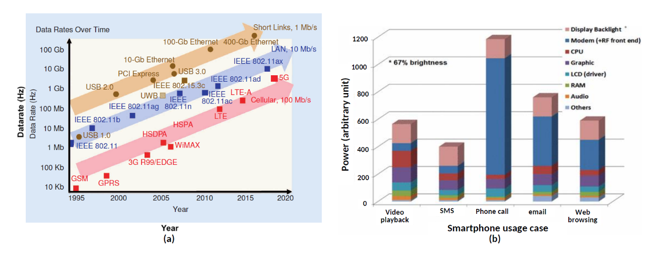
With the unending evolution of wireless communications and unceasing growth of RF system-on-chip (SoC) market, power-efficient frequency synthesis solutions with higher spectral purity, lower power and better robustness are more crucial than ever. Increasingly stringent specifications are imposed on integrated phase noise (IPN) and spur levels to fulfill related requirements, such as transmitter error vector magnitude (EVM), receiver sensitivity, and blocker tolerance. For instance, the ever-growing quests for higher data rates (Fig. (a)) have led to the utilization of dense constellations, such as 256-QAM (5G NR) and even 1024-QAM (802.11ax). Meanwhile, power consumption is another important concern as these handsets operate on batteries. As indicated by Fig. (b), the RF front-end consumes significant power for typical use cases of mobile terminals such as phone calls and web surfing. Furthermore, the frequency synthesis, leveraged as LOs in RF transceivers, consumes significant power compared to the total budget. Therefore, the main goal of the research is to seek an alternative and innovative way of frequency synthesis by phaselocked architecture, that demonstrates better performance at a lower cost with lower power.
Neural signal can be widely used for diagnosing the disease. For measuring the neural signal, the previous work such as medical instruments has difficulty to measure the signal inside of the body due to its bulkiness.
Neural recording IC enables to measure the signal inside of the body thanks to its compactness and low power.
There are interference for the neural recording IC such as current stimulation noise. Interference-robust neural recording IC can measure the neural signal more reliably regardless of the existence of the interference.
In wireline link, energy efficiency is a figure of merit that is given as ratio between total energy consumption and data-rate. It defines how much energy is consumed for communication between transmitter and receiver to send and recognize the bit data respectively.
However, due to ever increasing throughput and complexity in signaling method, competitive number for energy efficiency is challenging.
In this research, transceiver architecture and circuit techniques are proposed to achieve the best energy efficiency in wireline link.
Large portion of energy consumption in wireline transceiver circuit is from clocking, serializer and output driver from transmitter side, DSP engine for equalization and data post processing in receiver side. Also, the requirement of impedance matching between transmitter and receiver consumes significant power. In this research, transceiver architecture and circuit techniques are proposed to relieve the energy consumption in the core blocks of wireline transceiver.
The goal of this research is to propose and verify ultra-low power transceiver that achieves state-of-the-art energy efficiency in the field of wireline link.
VLSI 2018
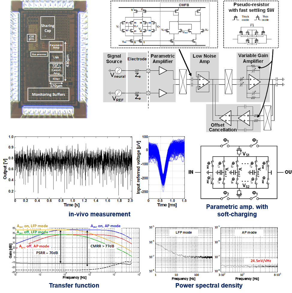
Neural recording sensor systems require miniaturization to limit brain tissue damage and accommodate tightly spaced electrodes. At the same time, neural potential sensor interface circuits must achieve aggressive input referred noise levels to monitor neural signals with sufficient accuracy. Given the small size and close proximity to sensitive brain tissue, power consumption is also highly constrained to meet strict tissue heating limits. In this work, we propose a new neural recording amplifier that achieves an NEF of 2.2 while meeting aggressive specifications such as > 100MΩ input impedance, > 70dB power supply rejection and common mode rejection ratios. We use a pre-amplifier stage that performs discrete-time parametric amplification based on MOS C-V characteristics. The sampling-induced kT/C noise is minimized by oversampling the input signal. The resulting power overhead is limited with stepwise charging and discharging of the source voltage in the parametric amplifier. Altogether, the design achieves the lowest-reported NEF among neural amplifiers while consuming 5.5uW with 1Hz – 8kHz bandwidth.
ISSCC 2016 JSSC 2018
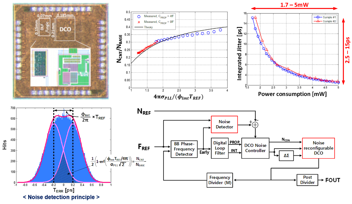
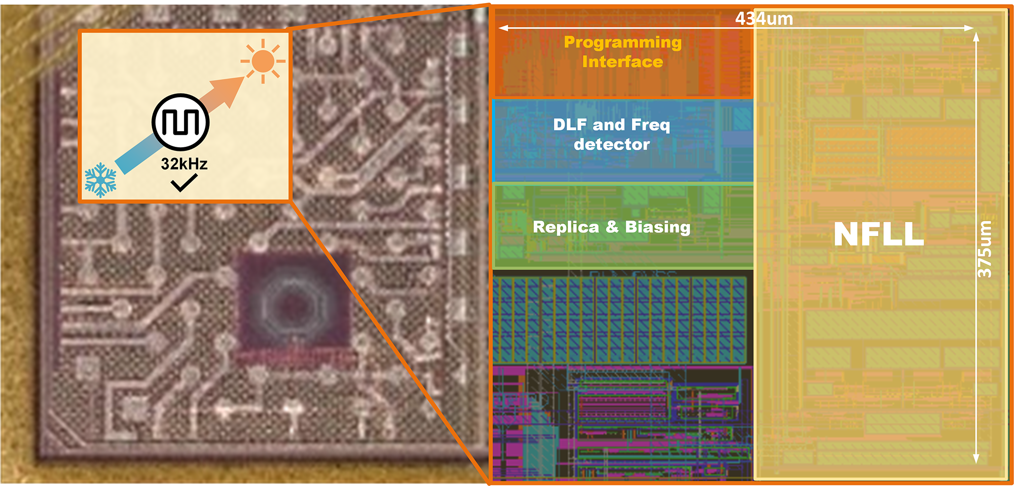
Digital PLLs are now popular for on-chip clock generation due to their small size and technology portability. Variability tolerance is a key design challenge when designing the PLLs in an advanced CMOS technology. Environmental variations such as mismatch, process, supply voltage, and temperature (PVT) perturb device characteristics and result in a change in the performance, such as DCO gain and noise. This work proposed a nested frequency locked-loop (FLL) architecture whose gain is accurately controlled by a capacitor ratio in order to keep the PLL bandwidth insensitive to variations.The noise of the FLL is programmable independently to the oscillation frequency. A noise detector block, using statistical characteristics of a bang-bang PFD (BBPFD) output, is proposed to efficiently sense DCO noise. The proposed PLL dynamically reconfigures the DCO noise from 2.5 to 15ps and self-adjusts its power from 1.7 to 5 mW according to the noise specification.
TCAS-I 2017
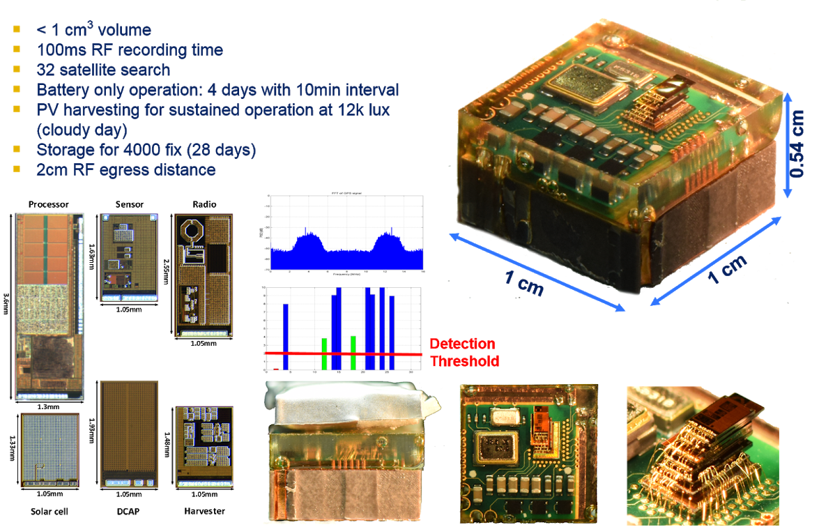
< 1 cm3 volume
100ms RF recording time
32 satellite search
Battery only operation: 4 days with 10min interval
PV harvesting for sustained operation at 12k lux (cloudy day)
Storage for 4000 fix (28 days)
2 cm RF egress distance
ISSCC 2016
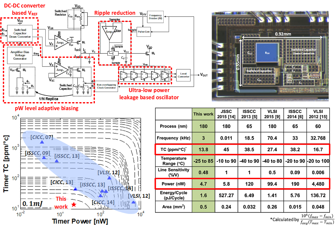
Miniaturized computing platforms typically operate under restricted battery capacity due to their size. Due to low duty cycles in many sensing applications, sleep mode power can dominate the total energy budget. Wakeup timers are a key always-on component in such sleep modes and must therefore be designed with aggressive power consumption targets (e.g., <10nW). Also, accurate timing generation is critical for peer-to-peer communication between sensor platforms. Although a 32kHz crystal oscillator can provide low power and accurate long-term stability, the requirement of an off-chip component complicates system integration for small wireless sensor nodes (WSNs).
To address this challenge and achieve a WSN timer with single-digit nW power consumption, we propose a new timer using a duty-cycled resistor scheme to increase resistance without impacting area. By generating the duty cycle using the frequency from the timer itself, an accurate on/off ratio is ensured. In addition, a current-reuse scheme is proposed to save power and also eliminates the need for chopping the bias current. Finally, a self-biasing technique is proposed to ensure stable operation and low power consumption across process-voltage-temperature (PVT) variations. Using these techniques, the timer achieves 13.8ppm/°C (−25 to 85°C) at 3kHz and consumes 4.7nW while showing less than 1.5× power variation across temperature.

A 4.1W/mm2 Power Density Fully Integrated DC-DC converter
Over the past years, the constant reduction in the size of consumer electronics has strengthened the demand for fully integrated power management circuits. This work proposes a new fully integrated DC-DC converter topology based on electromagnetically coupled class-D LC oscillators with on-chip transformers and flying capacitors. It relies on adiabatic switching of both the gate and bottom plate parasitic capacitances, allowing up to 3.15GHz switching frequency for aggressive scaling of the on-chip inductors and capacitors achieving 4.1W/mm^2 power density from a very compact 0.33mm^2 total chip area. Furthermore, the output power is delivered continuously by means of both magnetic and electric couplings, thus providing <1% output voltage ripple. The switch control signals are naturally provided by the self-oscillating nature of the converter, thus eliminating the area and power overhead of phase generator, level shifter and bootstrap auxiliary circuits. Finally, a duty cycling scheme improves the efficiency in light loads which remains close to the peak with less than 1% degradation from 0.003W/mm2 up to 2.1W/mm2 of output power density.
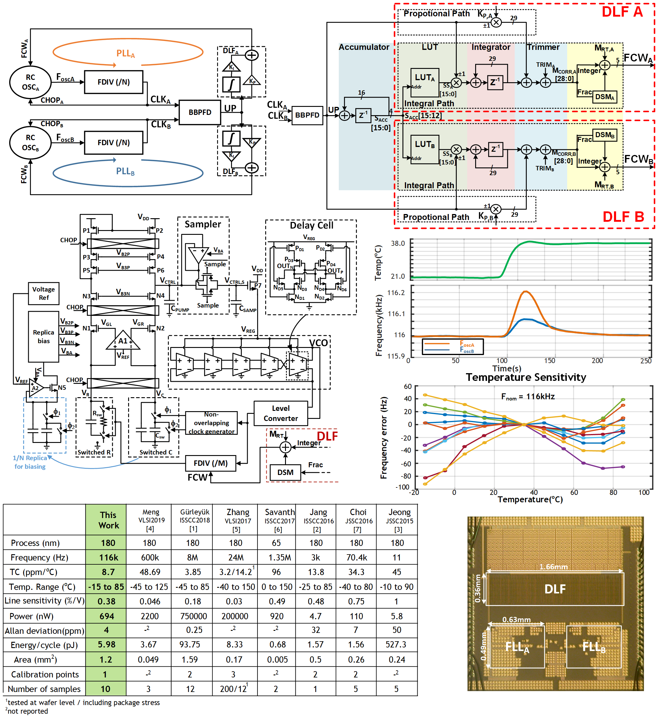
A precise timing reference is one of the key elements for digital systems, analog front-ends, communication systems and wireless sensor nodes. A monolithic on-chip oscillator is an attractive choice for the reduction of system volume, power consumption and cost.
The proposed design is an ultra-low-power on-chip timer which is resilient to temperature variation across a wide temperature range. The timer employs DSM-controlled RC oscillators and a non-linearity-aware digital dual phase-locked loop. The two oscillators equipped with different types of resistors generate different temperature-dependent periods. The dual PLL equalizes the frequencies of the two FLLs by adopting an integral path gain proportional to the oscillators’ temperature coefficients, so to achieve insensitivity to temperature. The proposed design can achieve 5.86ppm/°C while consuming 0.49μW.

Miniaturized low-power wireless systems equipped with sensing, computing and communication capabilities enable a wide variety of applications in the IoT era, ranging from environmental monitoring to healthcare. In this context, maximizing the energy efficiency while preserving the desired performance is a critical design issue, as the available energy is strictly limited by the requirements on the form factor. At the same time, mm-sized medical devices that have recently opened new frontiers for the treatment of several neurological disorders (e.g., epilepsy, Alzheimer, Parkinson’s disease) also suffer from a very limited power budget, arising from rigid safety regulations on the maximum heat dissipation in human tissue. These applications pose severe requirements on the input-referred noise (IRN) of the sensor-interface circuits, as the system receives a µV-level electrical signal from the sensor. Consequently, the low-noise amplifier (LNA), adopted as the first stage of the analog front-end (AFE), typically dominates the overall power consumption because it suffers from the most stringent input-referred noise specification.
We presented an energy-efficient low-noise amplifier, achieving 0.89 noise efficiency factor (NEF) using discrete-time parametric amplification. The power consumption is reduced by adopting a 34-phase stepwise charging technique and the sampling-induced input-referred noise is minimized by oversampling the input signal. Time-interleaving multiple parallel stages allows implementing the multiphase soft-charging scheme without causing any significant penalty in terms of area. A second current-reuse inverter-based amplification stage is designed to provide high gain, while its contribution to the total input-referred noise is attenuated by the preamplifier gain. The overall NEF is 1.76 and the total power consumption is 1.73 µW
Sound activity detection is a hot topic in consumer and smart city applications. One of the main applications in this area is keyword spotting of human sound that can serve as a natural user interface with IoT devices.
To achieve this goal, we are designing an analog front end of the acoustic sensor to detect the sound if existed and wake up the circuit for further processing of the sound and its detection. Our main challenges in this project besides from the power consumption and accuracy, which are the two most important targets, is the time of detection that shows the agility of our sensor.
